1. Black phosphorous and van de Waals heterostructure based THz nanodetectors
By exploiting the inherent electrical and thermal in-plane anisotropy of a flexible thin flake of black-phosphorus (BP), we recently devised plasma-wave, thermoelectric and bolometric nano-detectors with a selective, switchable and controllable operating mechanism. All devices operates at room-temperature, are based on SiO2-encapsulated BP flakes or hBN/BP/hBN hetrostructures and are integrated on-chip with planar nano-antennas, which provide remarkable efficiencies through light-harvesting in the strongly sub-wavelength device channel. The achieved selective detection (5-10 V/W responsivity) and sensitivity performances (signal-to-noise ratio of 20000), are here exploited to demonstrate the first concrete application of a phosphorus-based active THz device, for pharmaceutical and quality control imaging of macroscopic samples, in real-time and in a realistic setting.
More recently, we also devised Se-doped BP THz frequency nanodetectors showing a remarkable stability and state of the art sensitivity and noise performances.

(a) Sketch of a black phosphorus (BP) photodetector device structure (vertical section). (b) False colors SEM image of the BP-based FET. (c) Optical image of exfoliated flakes of BP. (d) Atomic force microscopy topographic image of an individual BP flake with thickness 6.2 nm. A topographic line profile, acquired along the dashed green line is shown. (e) Gate bias dependence of the experimental room temperature responsivity. The red line was measured by impinging the THz beam on the detector surface; the black line was measured while blanking the beam with an absorber (considering unaltered the incident power).
References:
1. L. Viti, J. Hu, D. Coquillat, A. Politano, C. Consejo, W. Knap & M.S. Vitiello, “Heterostructures hBN-BP-hBN Nanodetectors at terahertz frequencies” Adv. Mater. 28, 7390 (2016).2. L. Viti, J. Hu, D. Coquillat, A. Politano, W. Knap & M.S. Vitiello, “Efficient terahertz detection in black-phosphorous nano-transistors with selective and controllable plasma-wave, bolometric and thermoelectric response” Sci Rep. 6, 20474 (2016).3. L. Viti, A. Politano, K. Zhang & M.S. Vitiello, “Thermoelectric terahertz photodetectors based on selenium-doped black phosphorus flakes” Nanoscale, 11, 1995 (2019).4. L. Viti, A Politano & M.S. Vitiello, “Black phosphorous nanodevices at terahertz frequencies: Photodetectors and future challenges” APL Materials 5, 035602 (2017).5. A. Politano, M.S. Vitiello, L. Viti, J. Hu, Z. Mao, J. Wei, G. Chiarello & D. W Boukhvalov, “Unusually strong lateral interaction in the CO overlayer in phosphorene-based systems” Nano Res. 9, 2598 (2016).6. L. Viti, J. Hu, D. Coquillat, W. Knap, A. Tredicucci, A. Politano & M.S. Vitiello, “Black Phosphorous Terahertz Photodetectors” Adv. Mater. 27, 5567 (2015).
2. Plasma-wave THz detection mediated by Topological Insulators Surface States
As a very intriguing alternative, we explored Topological Insulator (TIs) which represent a novel quantum state of matter, characterized by edge or surface-states, showing up on the topological character of the bulk wave-functions. Allowing electrons to move along their surface, but not through their inside, they emerged as an intriguing material platform for the exploration of exotic physical phenomena, somehow resembling the graphene Dirac-cone physics, as well as for exciting applications in optoelectronics, spintronics, nanoscience, low-power electronics and quantum computing. Investigation of topological surface states (TSS) is conventionally hindered by the fact that, in most of experimental conditions, the TSS properties are mixed up with those of bulk-states. We devised a novel tool to unveil TSS and to probe related plasmonic effects. By engineering Bi2Te(3-x)Sex stoichiometry, and by gating the surface of nanoscale field-effect-transistors, exploiting thin flakes of Bi2Te2.2Se0.8 or Bi2Se3, we recently provided the first demonstration of room-temperature Terahertz (THz) detection mediated by over-damped plasma-wave oscillations on the “activated” TSS of a Bi2Te2.2Se0.8 flake.
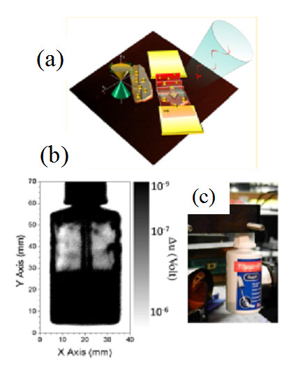
(a) Schematic sketch of a THz detection process mediated by topological insulator surface states. (b) Room temperature, large area THz imaging obtained while impinging the 332.6 GHz radiation a topological insulator THz detector, mounted on a XY stage, with an acquisition time of 20 ms/pixel. For visible light illumination the contents cannot be seen, either by naked eye or by the CCD camera used to take the picture. The detection of THz transmitted radiation gives information about the jar content. (c) Photograph of the glue jar.
References:
1. L. Viti , D. Coquillat, A. Politano, K.A. Kokh, Z.S. Aliev, M.B. Babanly, O.E. Tereshchenko, W. Knap, E.V. Chulkov & M.S. Vitiello, “Plasma-Wave Terahertz Detection Mediated by Topological Insulators Surface States” Nano Lett. 16, 80 (2016).2. A. Politano, V.M. Silkin, I.A. Nechaev, M.S. Vitiello, L Viti, Z.S. Aliev, M.B. Babanly, G. Chiarello, P.M. Echenique & E.V. Chulkov, “Interplay of surface and Dirac plasmons in topological insulators: the case of Bi2Se3” Phys.Rev. Lett. 115, 216802 (2015).3. A. Politano, M.S. Vitiello, L. Viti, D.W. Boukhvalov & G. Chiarello, “The role of surface chemical reactivity in the stability of electronic nanodevices based on two-dimensional materials “beyond graphene” and topological insulators” FlatChem 1, 60 (2017).
3. Semiconductor nanowire THz detectors
The recent progresses in atomic to nanometer scale control of materials morphology, size, and composition including the growth of axial, radial and branched nanowire-based heterostructures, make the nanowire (NW) an ideal building block for implementing rectifying diodes or detectors that could be well operated into the Terahertz (THz), thanks to their typical achievable attofarad-order capacitance. We recently devised 1D InAs or InAs/InSb NW-based field effect transistors (FETs) exploiting novel morphologies and/or material combinations effective for addressing the goal of a semiconductor plasma-wave THz detector array technology. We demonstrated room-temperature operation in the 0.3-3 THz range with over 100V/W responsivity and < 1nW/Hz1/2 noise equivalent powers.
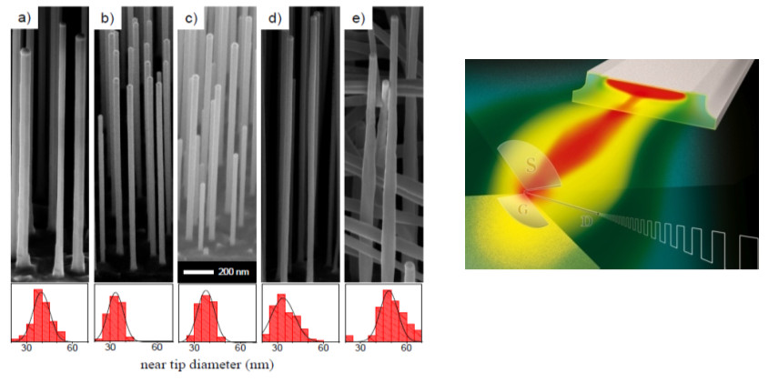
(Samples a, b, c, d, and e) 45° tilted SEM image of the investigated InAs nanowires. Right panel: schematics of the nanowire detection of THz frequency light.
References:
1. M.S. Vitiello, L. Viti, D. Coquillat, W. Knap, D. Ercolani & L. Sorba, “One dimensional semiconductor nanostructures: An effective active-material for terahertz detection“ APL Materials 3, 026104 (2015).2. M.S. Vitiello, L. Viti, L. Romeo, D. Ercolani, G. Scalari, J. Faist, F. Beltram, L. Sorba & A. Tredicucci, “Semiconductor nanowires for highly sensitive, room temperature detection of terahertz quantum cascade laser emission” Appl. Phys. Lett. 100, 241101 (2012).3. M.S. Vitiello, D. Coquillat, L. Viti, D. Ercolani, F. Teppe, A. Pitanti, F. Beltram, L. Sorba, W. Knap & A. Tredicucci, “Room-Temperature terahertz detectors based on semiconductor nanowire field-effect transistors“ Nano Lett. 12, 96 (2012).4. L. Romeo, D. Coquillat, E. Husanu, D. Ercolani, A. Tredicucci, F. Beltram, L. Sorba, W. Knap & M.S. Vitiello, “Terahertz photodetectors based on tapered semiconductor nanowires“, Appl. Phys. Lett. 105, 231112 (2014).
4. Graphene THz ultrafast detectors
By exploiting the unique ability of graphene to efficiently convert absorbed light (of any wavelength) into hot graphene electrons we develop ultrafast graphene detectors at terahertz frequencies, exploiting a high dynamic range and broadband operation over the 1.2 – 5 THz range.
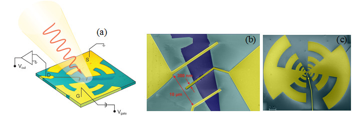
(a) Device schematics; (b-c): SEM images of the antenna embedded single layer graphene THz FET detector.
References:
1. F.H.L. Koppens, T. Mueller, Ph. Avouris, A.C. Ferrari, M.S. Vitiello & M. Polini, “Photodetectors based on graphene, other two-dimensional materials and hybrid systems”, Nat. Nanotechnol. 9, 780 (2014).2. L. Vicarelli, M.S. Vitiello, D. Coquillat, A. Lombardo, A.C. Ferrari, W. Knap, M. Polini, V. Pellegrini & A. Tredicucci, “Graphene field-effect transistors as room-temperature terahertz detectors”, Nat. Mater. 11, 865 (2012).
5. THz detection of magnetic field-driven topological phase transition in HgTe-based transistors
We demonstrated terahertz detection by inverted band structure HgTe-based Field Effect Transistor up to room temperature. At low temperature, we show that nonlinearities of the transistor channel allows for the observation of the quantum phase transition due to the avoided crossing of zero-mode Landau levels in HgTe 2D topological insulators. These results pave the way towards THz topological Field Effect Transistors.
References:
1. A.M. Kadykov, F. Teppe, C. Consejo, L. Viti, M.S. Vitiello, S.S. Krishtopenko, S. Ruffenach, S.V. Morozov, M. Marcinkiewicz, W. Desrat, D. Dyakonova, W. Knap, V.I. Gavrilenko, N.N. Mikhailov, S.A. Dvoretsky, “Terahertz detection of magnetic field-driven topological phase transition in HgTe-based transistors”, Appl. Phys. Lett. 107, 152101 (2015).