1. Near field THz probes
Near-field imaging with terahertz (THz) waves is emerging as a powerful technique for fundamental research in photonics and across physical and life sciences. Spatial resolution beyond the diffraction limit can be achieved by collecting THz waves from an object through a small aperture placed in the near-field. However, light transmission through a sub-wavelength size aperture is fundamentally limited by the wave nature of light. We conceived a novel architecture that exploits inherently strong evanescent THz field arising within the aperture to mitigate the problem of vanishing transmission. The sub-wavelength aperture is originally coupled to asymmetric electrodes, which activate the thermo-electric THz detection mechanism in a transistor channel made of flakes of black-phosphorus or InAs nanowires. The proposed novel THz near-field probes enable room-temperature sub-wavelength resolution coherent imaging with a 3.4 THz quantum cascade laser, paving the way to compact and versatile THz imaging systems and promising to bridge the gap in spatial resolution from the nanoscale to the diffraction limit.
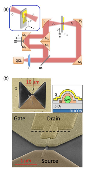
(a) Schematics of the interferometric THz near-field microscopy setup. The inset shows the near-field probe geometry. (b) (upper left and lower left) Scanning electron microscope (SEM) images of the near-field probe with an embedded FET-based THz nanodetector (view angles of 0° and 70°). (b) (upper right) Schematic diagram of the cross-sectional view of the detector.
References:
1. M.C. Giordano, L. Viti, O. Mitrofanov & M.S. Vitiello, “Phase-sensitive terahertz imaging using room-temperature near-field nanodetectors” Optica 5, 651 (2018).2. O. Mitrofanov, L. Viti, E. Dardanis, M.C. Giordano, D. Ercolani, A. Politano, L. Sorba & M.S. Vitiello, “Near-field terahertz probes with room-temperature nanodetectors for subwavelength resolution imaging” Sci Rep. 7, 44240, (2017).
2. Near field detectorless s-SNOM THz microscopy
At terahertz (THz) frequencies, scattering-type scanning near-field optical microscopy (s-SNOM) mostly relies on cryogenic and bulky detectors, which represents a major constraint for its practical application. In the first 18th months we devised a THz s-SNOM system that provides both amplitude and phase contrast, and achieves nanoscale (60-70 nm) in-plane spatial resolution. It features a quantum cascade laser that simultaneously emits THz frequency light and senses the backscattered optical field through a voltage modulation induced inherently through the self-mixing technique. We demonstrated its performance by probing a phonon-polariton-resonant CsBr crystal, doped black phosphorus flakes and ink jet printed graphene.

Self-detection scattering type near field optical microscope with nanometer resolution at terahertz frequencies. (a) Schematic diagram showing the experimental arrangements.
References:
1. M.C. Giordano, S. Mastel, C. Liewald, L.L. Columbo, M. Brambilla, L. Viti, A. Politano, K. Zhang, L. Li, A.G. Davies, E.H. Linfield, R. Hillenbrand, F. Keilmann, G. Scamarcio & M.S. Vitiello, “Phase-resolved terahertz self-detection near-field microscopy” Optics Express 26, 18423 (2018).
3. Ultrafast near-field THz nano-spectroscopy
We extend ultrabroadband time-resolved terahertz spectroscopy to the sub-nanoparticle scale (10 nm) by combining subcycle, field-resolved detection (10 fs) with scattering-type near-field scanning optical microscopy. We trace the time-dependent dielectric function at the surface of a single photoexcited InAs nanowire in all three spatial dimensions and reveal the ultrafast (<50 fs) formation of a local carrier depletion layer.
We also applied the above technique to demonstrate that black phosphorus is as a promising new material in surface polaritonics that features key advantages for ultrafast switching. We designed a SiO2/black phosphorus/SiO2 heterostructure in which the surface phonon modes of the SiO2 layers hybridize with surface plasmon modes in black phosphorus that can be activated by photo-induced interband excitation.We find that the surface mode can be activated within ∼50 fs and disappears within 5 ps, as the electron–hole pairs in black phosphorus recombine. The excellent switching contrast and switching speed, the coherence properties and the constant wavelength of this transient mode make it a promising candidate for ultrafast nanophotonic devices.
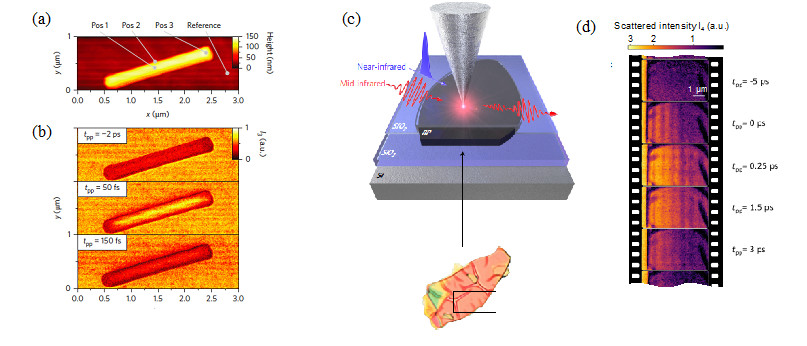
(a) Ultrafast THz nano-movie frames of nanowire photoexcitation. Free carriers are photoinjected into the InAs nanowire by near-infrared pump pulses and time-resolved near-field THz intensity images are measured as a function of pump–probe delay time. (b) Top: schematic of set-up. An ultrafast near-infrared pump pulse is focused onto a heterostructure of SiO2 and BP on a SiO2-capped Si wafer. The sample is probed in the near field with a mid-infrared pulse coupled to a sharp metallic tip. Bottom: optical image of a single BP flake capped with SiO2. (c) Scattered near-field intensity images of the SiO2/BP/ SiO2 heterostructure, plotted for different delay times between the pump and probe pulses.
References:
1. M.A. Huber, F. Mooshammer, M. Plankl, L. Viti, F. Sandner, L.Z. Kastner, T. Frank, J. Fabian, M.S. Vitiello, T.L. Cocker & R. Huber, “Femtosecond photo-switching of interface polariton in black phosphorous heterostructures”, Nat. Nanotechnol. 12, 207 (2017).2. M. Eisele, T. L. Cocker, M. A. Huber, M. Plankl, L. Viti, D. Ercolani, L. Sorba, M. S. Vitiello & R. Huber, “Ultrafast multi-terahertz nano-spectroscopy with sub-cycle temporal resolution”, Nat. Photonics 8, 841, (2014).3. A. Agarwal, M.S. Vitiello, L. Viti, A. Cupolillo & A. Politano, “Plasmonics with two-dimensional semiconductors: from basic research to technological applications” Nanoscale 10 , 8938 (2018).